

A 2D quantum interfacial doping effect for 3D complementary logic
source:admin update time:2024-05-29 15:43:00


[Decades of Development and the Path Beyond Moore's Law]
Over decades of advancement, semiconductor manufacturing processes have continuously approached the sub-nanometer physical limit. Traditional silicon-based integrated circuits can no longer rely solely on scaling down transistor dimensions to sustain Moore's Law. Developing vertically structured, multi-layer interconnected complementary logic circuits (CMOS) to achieve breakthroughs in upward integration has emerged as a key new direction actively pursued by the global semiconductor industry. For instance, at the 2023 International Electron Devices Meeting (IEDM) in San Francisco, leading semiconductor companies such as Samsung and TSMC competed to unveil related research initiatives.
[The Limitations of Silicon-Based Transistor Technology]
Silicon-based transistor fabrication relies on ion implantation into single-crystal silicon surfaces, making it extremely difficult to grow or transfer another layer of single-crystal silicon on top. While 3D integration techniques—such as interconnecting electrodes or chiplets—can improve density, the critical transistors remain confined to the bottom layer, lacking true "Z-direction" freedom. This fundamental constraint has driven intense interest in new materials and disruptive physical principles as potential breakthroughs.
[A Quantum-Enabled Breakthrough in 2D Semiconductor Doping]
A collaborative team from the Institute of Quantum Materials & Devices at the Liaoning Academy of Materials, along with domestic and international partners, has proposed a p-type doping method for 2D semiconductors based on interface coupling, where theoretical evidence indicates quantum effects play a decisive role. This approach leverages an interface-driven mechanism, offering simple processing, exceptional stability, and preservation of the 2D semiconductor’s intrinsic superior properties. Building on this innovation, the team successfully fabricated vertically stacked complementary logic gates (NAND and SRAM) composed of 14 layers of van der Waals materials and 4 transistors, as illustrated in Figure 1.
[Breaking the Silicon Barrier: A New Era for 3D Integration]
This work may find applications beyond the limitations of silicon-based logic circuits, demonstrating 3D vertically integrated multi-layer complementary transistor arrays enabled by quantum effects. It provides a transformative strategy for advancing post-Moore 2D semiconductor devices.
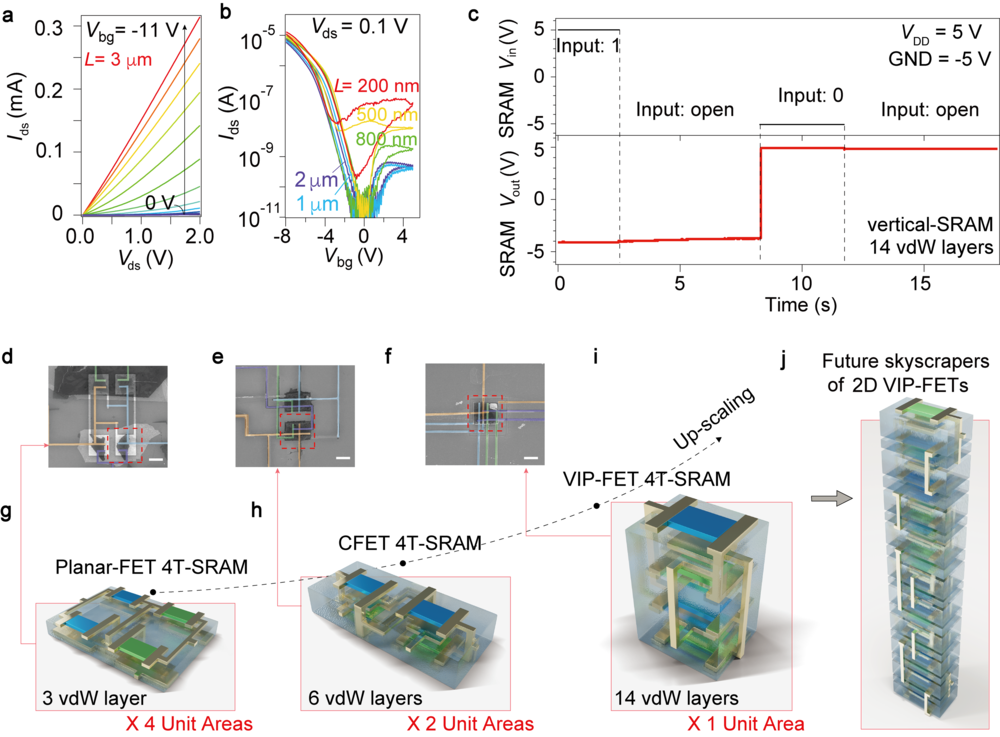
Fig. 1. Vertical integration of 2D semiconductors into 3D logics.
Read the research paper:https://www.nature.com/articles/s41586-024-07438-5
- Research Highlights